PCB Layout Process
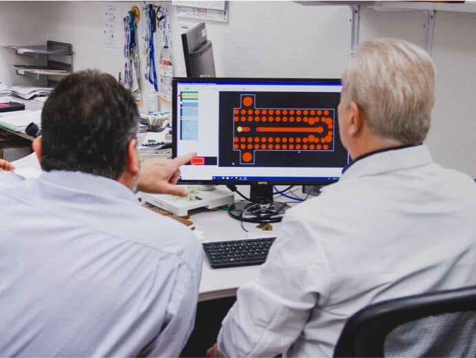
This is where your printed circuit board begins. At the PCB layout stage, we work with principal engineers and fellows to develop a layout with a software platform such as Mentor® PADS, which shows you exactly how your board will look and where the components will be placed.
Our process of working with our clients from the beginning to develop and produce the best possible custom-printed circuit board is known as concurrent engineering. Throughout the layout process, our proficient engineers provide recommendations on material stackups to meet impedance requirements and how to design for manufacturability. Our involvement from the start ensures your PCB is designed and manufactured correctly — without the need for multiple revisions.
Let our PCB team initiate the process of seamless integration as your project advances from layout all the way through fabrication and assembly — all under one roof in our state-of-the-art facility. Plus, if we’re involved throughout the entire process, your PCB will often hit the market faster when you use one vendor.

