Your Guide to Flexible PCB Design & Layout

All printed circuit boards essentially perform similar functions, but there are three main types — rigid, rigid-flex, and flex — which all differ in terms of design and construction. As you might be able to tell from their names, rigid boards don’t bend, while flex PCBs can be shaped and designed to fit into certain products or systems. A rigid-flex board is a combination of the two.
In this comprehensive guide on flexible PCB design, we’ll cover everything you need to know when it comes to flex and rigid-flex boards, including the types of flex circuits, benefits, commonly used materials, cost drivers, and a step-by-guide.
Types of Flexible Circuits
- Flex: A flex, or flexible, circuit is a made of thin, flexible material. Applications for flex circuits might be as simple as a one layer circuit. A multilayer printed wiring circuit board contains three or more copper conductive layers usually with plated through holes.
- Rigid-flex: If the multilayer circuit board is constructed of both flexible and rigid materials, it’s referred to as a rigid-flex circuit board. A rigid-flex circuit board is a 3D interconnect that can be bent and folded into almost any shape. Rigid-flex technology allows designers to replace multiple PCBs with interconnecting wires and/or cables into one single unit, offering improved performance and increased readability. Rigid-flex circuits can have up to 50 layers, replacing bulky wire harnesses with a compact, robust design.
- High density interconnect: HDI rigid-flex PCBs are characterized by a higher layer count, thin lines, closer spaces, and more dense wiring, with features that allow for a faster connection while reducing the size and bulk of a project. These boards also feature blind and buried vias, laser-drilled microvias, sequential lamination, and via in-pads.
8 Benefits of Flexible Circuits
Flex circuits offer numerous benefits that make them ideally suited for designs where saving weight and space and incorporating complex design movement are critical. These benefits include:
1. Repeatable reliability
A flex circuit allows you to customize a routing path within your printed circuit board, which provides enhanced reliability and dependability.
2. Withstands tough environments
The materials used ensure that flex circuits can withstand a full spectrum of gravitational force, and taxing conditions — from dropping your cell phone to the launch of a missile.
3. Survives high temperatures
Flex circuits are able to endure higher temperatures, which makes them ideal for a wide variety of industries, including aerospace, military, down hole oil, and medical.
4. Long-duty cycles
A flex circuit’s durability means it can tolerate a large volume of flexing cycles while carrying signal and power without disruption.
5. High vibration
Flex circuits have low mass and are ductile, which means they can undergo a significant strain or shape change without breaking or losing strength. As a result, flex circuits can withstand high vibrations.
6. Space saving
Flex circuits allow you to save space by replacing large amounts of wiring and cables. This also makes them lightweight, which means they can reduce the overall weight of a package significantly. From surgical tools and cell phones to equipment and automobile car seats. Flex circuits can also conform to a wide variety of spaces, and applications.
7. Improved signal integrity
Flex circuits are ideally suited to high-speed digital signaling systems where signal integrity is essential. In practice, high speed basically means rapid rise times, and anything that degrades the ideally square wave pulse signal must be managed.
8. Decrease in assembly time, cost, and errors
Flex circuits have the ability to seamlessly integrate form, fit, and function of a design into a single circuit. This means flex circuits can offer an effective way to reduce the cost of assembly of the final product. In turn, reducing assembly steps also reduced the potential for errors.
Common Materials in Flexible Circuits
The most common materials in flex circuits include:
Conductor
Copper foil is the most commonly used material because it’s extremely conductive. You also don’t have to use a lot of copper in order for the PCB to be effective. It’s also available as fully annealed or low temperature annealed, which provides better flexing characteristics.
Insulator and coverlayer
Polyimide film is the most commonly used dielectric and insulator. It’s also used as the coverlayer, which insulates the copper conduct as the outside layer of the flex circuit.
Finish type
A PCB surface finish has two main functions: To prevent the copper from oxidizing and to provide a solderable surface. One of the most common finishes is Electroless Nickel Immersion Gold (ENIG), which is used on about 80% of all boards. This finish provides a thin, solderable, gold layer that protects the copper traces with a nickel barrier between it and the copper.
Electroless Nickel Electroless Palladium Immersion Gold (ENEPIG) is a three-layer metallic finished used for printed circuit boards that also require wire bonding. The electroless nickel protects the copper and prevents it from coming into contact with the other metals. Palladium provides another anti-oxidation insurance and wirebonding layer and prevents the nickel from corroding, and the final gold layer adds solderability capability and a barrier against oxidation.
Cost Drivers in Flexible Circuits
When you’re navigating a flexible PCB design, the goal is to create a cost-effective product without sacrificing performance. Here are some considerations to keep in mind that could add additional costs, depending on your project. As always, it’s best to consult with an engineering expert if you have questions.
Layer count
A flex circuit with many layers usually indicates a higher cost since additional materials and time will be required. Some of these multilayer projects may also prove technically challenging.
Circuit size and shape
The size and shape of flex circuits affect how many can be fit on a manufacturing panel, which affects the pricing.
Circuit type
Does your project need rigid-flex construction, or will a multilayer with stiffener work just as well? Rigid-flex circuits are usually more expensive.
Circuit class
What is the right IPC class for your flex circuit? Class 3 will demand more requirements requiring serialization and more coupons for validation than Class 2, which will drive up the cost of your project.
Different layer counts in plated through hole areas
Areas with plated through holes should have the same number of layers; differing layers can increase the cost.
Dimensional tolerances
Flex circuit materials allow and require looser tolerances than rigid PCBs, and each dimension will have to be verified. If a dimension isn’t essential to the project, it should be marked as a reference.
Multiple final finishes
As with layer counts, more of anything usually increases the cost — including finishes.
Small features
Is it more cost effective to add additional layers with larger features instead of smaller ones? It’s best to consult your PCB design and layout experts early in the process.
Blind and buried vias
Vias are an essential part of the multi-layered PCB design and manufacturing process. A vertical interconnect access (or via) is a plated through hole that is used to route a trace vertically in the board from one layer to another. These features are typically more expensive than through holes.
Step-by-Step Guide to Designing Flex Circuits
1. Understand the electrical parameters.
Before starting a flex PCB design, you should know and understand the electrical parameters of the system, including:
- Current maximums
- Voltages
- Signal types
- Capacitance limitations
- Impedance characteristics
- Shielding considerations
- Type and location of circuit components and connectors
- Detailed net wire listing and schematic
2. Create the schematic.
One of the first steps is always creating a schematic, which refers to the general representation, design, and shape of your circuit board. Tip: At this early stage, it’s important to think about the bendability of your PCB. Is your board static or dynamic? A dynamic board must be able to endure a lifetime of bending, as opposed to a static board, which may only bend a handful of times.
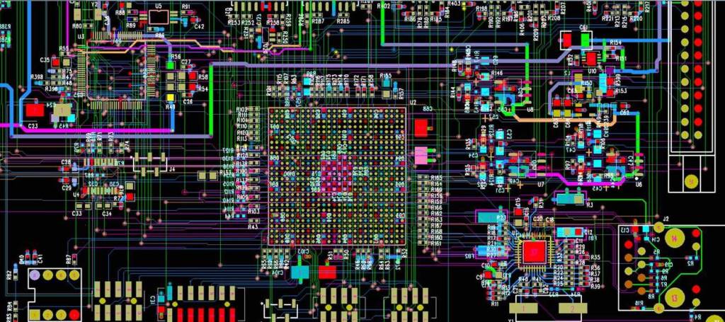
3. Use a schematic capture tool to create your PCB layout.
The right layout provider will work with principal engineers to develop a layout with a software platform such as Mentor® PADS, Allegro, or Altium, which shows you exactly how your board will look and operate and where the components will be placed. After you create your layout, the mechanical engineer will load the design and determine how it will fit in the intended device. Tip: It’s also important to think about flex PCB materials, which often require looser manufacturing outline tolerances than other boards.
4. Design your flex PCB stackup.
This is important to consider early on in the PCB design stage due to impedance, which refers to how much and how quickly electricity can travel down a trace. The stackup plays a role in how the EE and mechanical engineer can design and fit the PCB into the device. Tip: Place the flex layers in the middle of the stackup, which provides protection.
5. Define design rules and requirements.
This step is largely dictated by standards and acceptability criteria from IPC, which is the industry association for PCB and electronics manufacturing. These standards tell you everything you need to know regarding PCB manufacturing. Tip: Find a PCB layout provider who is extremely familiar with IPC standards; this can help you avoid major revisions and project delays.
6. Place your components.
In many cases, the customer and PCB/layout provider will discuss design and layout guidelines when it comes to the placement of components. For example, there may be standards indicating that certain components cannot be placed near others because they create electrical noise in the circuit. The layout provider will have data sheets on every component (in most cases these are connectors), which will then be placed in the mechanical layout and sent to the customer for approval.
7. Insert drill holes.
This step is driven by the components and a connection. About half of the flex circuits on the market are double-sided, which means they have connection to the drilled hole top to bottom layer.
8. Route the traces.
After you’ve placed the components and drill holes, you’re ready to route the traces, which means connecting segments of the path.
9. Add labels and identifiers.
Now is the time to add any labels, identifiers, markings, or reference designators to the layout. Reference designators are helpful in showing where specific components will go on the board.
10. Generate design/layout files.
This is the final step in the process with the software program. These files contain all the information pertaining to your flexible PCB design, and once they have been generated, your PCB is now ready for fabrication and manufacturing and assembly.
Key Considerations When Designing a Flex Circuit
From materials to vias, there are a lot of factors that go into designing a flex circuit. Here are some things to keep in mind as you consider your flexible PCB design:
- Operating environment: What is the environment in which the final product has to function? Is your flex circuit designed for a non-extreme environment, such as a cell phone, or the highest of extremes, such as an explosion?
- Bend ratio: This refers to the relation of bend radius to the thickness of the flex circuit. The tighter a bend radius becomes, the higher the probability of failure during flexing.
- Conductors and routing: This refers to the route that transmits the electrical current from one spot to another. The conductor pattern should also be analyzed to determine if it will be affected by the flexing. Conductors should always be routed through bend areas as close to perpendicular as possible.
- Pad fillets: These will improve etched yield and material strength and are appropriate when the pad diameter is greater than the connecting strand width.
- Tear relief: There are a few common ways of eliminating tears in a flex circuit, including a relief slot and large corner radius. It’s best to consult with the engineering experts to determine the best method for your project.
- Vias: Do you need blind or buried vias, which will likely increase the cost of your project?
- Surface Mount Access (SMT) access openings: Flex circuits can be made with areas that are specifically designed for surface mount components because coverlays are laser cut, not masked. Photo imageable coverlay materials are also available and can provide intricate, irregular shaped openings for dense surface mount patterns.
- Stiffeners: A mechanical stiffener can rigidize the SMT, connector, and other areas on your flexible PCB.
- Plane layers and shielding: Reference plane layers and shielding are extremely important when it comes to impedance control and signal integrity. As the common method of shielding, solid copper increases the rigidity of the circuit and should be included in the thickness-to-bend radius review. Other shielding methods can be used to increase flexibility, such as, cross hatching and Silver ink.
- Controlled impedance and signal integrity: Impedance refers to how much and how quickly electricity can travel down a trace. Matching impedance refers to the correct function of your signals and the overall circuit board. Certain factors will affect the impedance characteristic of a flex circuit, including relative permittivity of the insulation materials used, the width of the traces, the distance of the signal traces from the reference plane layers, the thickness of the traces, and the distance between trace signals in different impedance applications.
- Assembly considerations: There’s a lot to think about when actually assembling your flex circuit, but here are a few things to keep in mind as you navigate the design process:
- You want to make sure all moisture is removed before the circuit is subjected to high temperatures.
- Process the flex circuits immediately after baking. If this isn’t possible, store your circuits in a nitrogen chamber or a sealed dry box with desiccant.
Need Help from the Professionals?
Are you looking for help with your next flexible PCB design? Navigating the process can be a challenge, but we are here to help. Cirexx is your best-in-class solution for PCB layout. With more than four decades of experience, we have manufactured PCBs for almost every leading technology company – and we’ve worked with industries all over the world. Contact us today to learn more about our capabilities or to consult with one of our engineering experts on your next flexible PCB project.