PCB Vias [Your Full Guide]


Vias are an essential part of the multi-layered printed circuit board (PCB) design and manufacturing process – but what are they exactly? And how do the various kinds differ from one another? In this article, we’ll cover all the basics – including the via-making process, the most common types, and how you should choose the best vias for your next project.
What Is a PCB Via?
What Is a Via In-Pad?
What Is an Anti-Pad?
The Via-Making Process
The 4 Most Common Types of Vias
How to Choose the Right Via – Plus Design Tips
What Is a PCB Via?

A vertical interconnect access (or via) is a plated-through hole in a printed wiring board that is used to route a trace vertically in the board from one layer to another. Vias can be drilled mechanically or with a laser, and they are plated to form electrical connections.
Why are vias important? PCB vias are essential to multi-layer printed circuit boards, which can be a challenge to design and manufacture. The vias deliver a route through which electrical and thermal energy can move between layers. In other words, vias are essentially “channels” that can range in size and type.
What Is a Via In-Pad?
A via in-pad is a laser drilled plated hole that joins copper paths from one layer to another in order to create a better thermal or electrical connection.
You can have a laser drilled and potentially through hole drilled in-pad depending on the size of the pad.
What Is an Anti-Pad?
An anti-pad is the open space between the pad and copper layers that does not have a connection. Via anti-pads, which are also referred to as clearances, insulate the pad from the surrounding copper.
The Via-Making Process
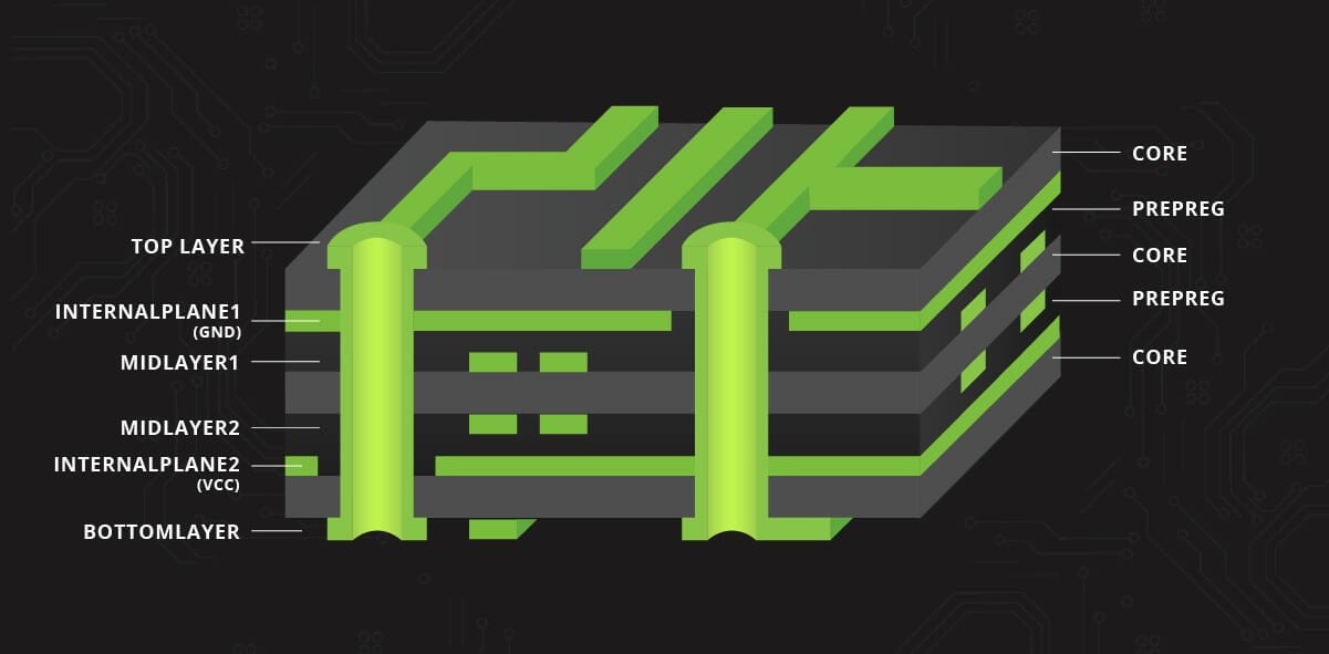
Mechanical vias contain a data package that illustrates the traces that will connect to the mechanically drilled hole, which will eventually become plated.
Laser-drilled vias and/or laser drilled via in-pads go from one layer to the next (or they could be in a stack of via structures). A laser drill through the copper and substrate will open the copper at the bottom of the hole, after which the hole can be plated closed. At that point, the top and bottom layers are connected without the need to drill a hole through the project.
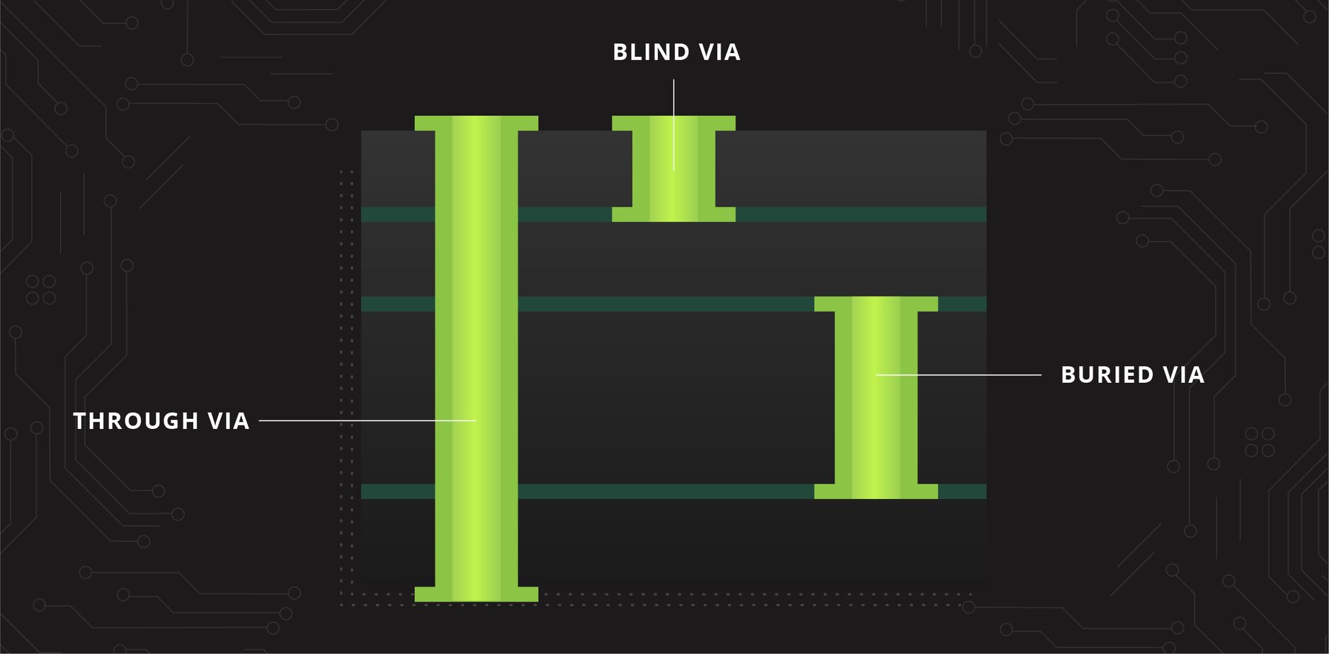
The 4 Most Common Types of PCB Vias
- Blind via: This type of via always refers to a laser that only goes from one layer to the next.
- Buried via: A buried via is needed when you have what is commonly referred to as sequential lamination (or multi-lamination) projects.
- Through via: A through via connects the two exterior layers by drilling all the way through from the top to bottom layer.
- Blind via in-pad: This via refers to a laser that only goes from one layer to the next.

6 Factors to Consider When Choosing the Right Via – Plus Design Tips
It’s important that you and your PCB solutions provider select the right via for your project – and that you understand design for manufacturability. Here are 6 factors to consider as you think about your next project:
- Via type. What would be best for your project: a buried, blind, or through via? If you have one lamination with no via fill or technology you will have a lot of room for larger holes.
- Via size. The most common via size is 10 mil, which would be a 7 mil after plating, but via size depends on the thickness of the board. It’s an aspect ratio equation. Micro vias, both laser drilled and mechanically drilled 4 mil holes, are related to the thickness of the boards.
- Via tolerance. It’s important to specify hole size tolerance, but PCB providers often provide in-house guidelines.
- Support the appropriate technology. When you need blind or buried vias, consult with your PCB supplier to begin developing a stack up that supports that technology.
- IPC guidelines. It’s essential to always follow IPC guidelines for the associated technology, which include stipulations such as distance between vias. IPC design guidelines for Class 2, Class 3, Class 3DS, and military are especially important because they all differ slightly.
- Annular ring. Be mindful of annular ring requirements per Class 2 and Class 3. An annular ring is what’s left after you drill through the pads of each layer. You are plating through the hole and drilling through the pad, and you still are making an electrical connection with copper, but you have a lot of tolerance to deal with when drilling vertically. You will have to deal with the tolerances of movement of materials and also how the drill plunges through the material. The annular ring provides enough land area in the internal areas to still maintain a copper connection to the trace on the particular layer before plating a through hole. In other words, it’s about assuring per Class 2 or Class 3 that you are maintaining an electrical connection and have the tolerance you need from the materials and the drill bit location.
Covering and Filling Vias
Filling a via must prevent the entrapment of chemicals or other substances within the holes, which can eventually cause defects to the printed circuit board. Vias are filled with conductive or non-conductive paste. Blind vias and via in pads are filled with specially designed electroplating.
If you are looking to move heat from one side of the printed circuit board to the other, you will likely opt for a conductive fill.
Vias must be sealed or covered by capped plating. The combination of the sequential build-up of technology and the mechanical processes can disturb the buried via plating, resulting in problems with the board. To prevent this problem, the vias are filled with resin before being plated.
A via in pad must be plated because you are putting in a component connection, and you can’t have a recess hole.
—
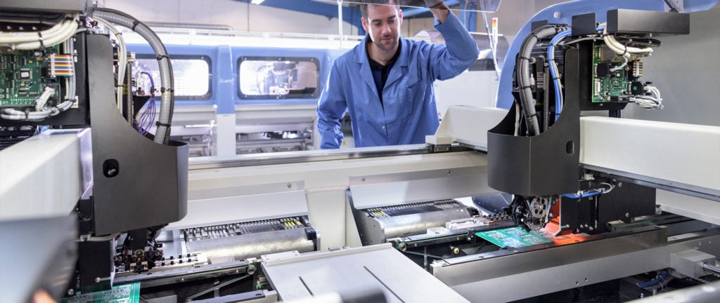
Cirexx is your best-in-class solution for PCB layout, fabrication, and assembly. With more than four decades of experience, we have manufactured PCB layouts for almost every leading technology company – and we’ve worked with industries all over the world. Contact us today to learn more about our high-value, end-to-end solution capabilities or to connect with our sales team.