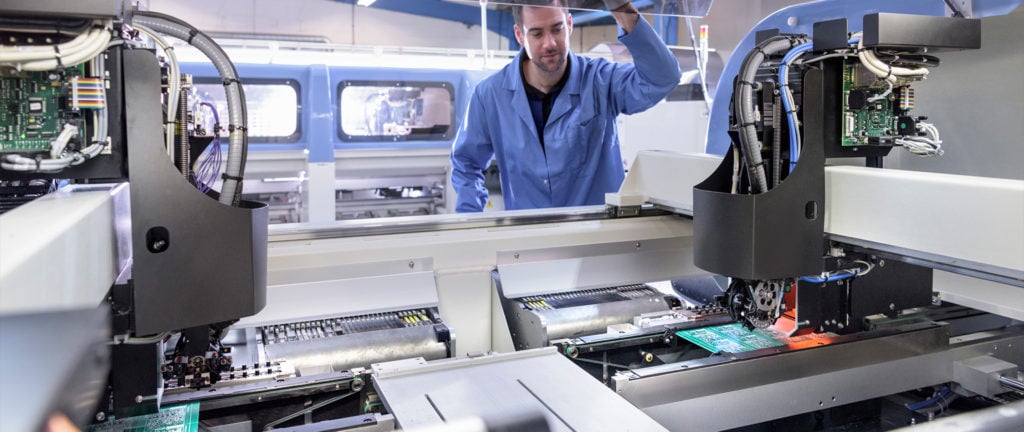
High-Speed PCB Design

It’s important to design a printed circuit board (PCB) correctly from the start, and a high-speed PCB is no exception. In this guide, we’ll cover everything you need to know about high-speed PCB design, include all the components of a successful design, a typical high-speed PCB stackup, and high-speed routing guidelines.
What is a High-Speed PCB?
Impedance in High-Speed PCB Design
Why is Design So Important in a High-Speed PCB?
High-Speed PCB Stackup
Developing a High-Speed PCB Schematic
Important Components in a High-Speed PCB Design
High-Speed PCB Design Guidelines
What is a High-Speed PCB?
High-speed refers to a printed circuit board with a high layer and signal count. These types of PCBs often involve processor speeds, DDR signals, and many differential signals.
How are high-speed PCBs different from high-frequency (HF) PCBs? HF PCBs are defined by low levels of thermal expansion and are used for high technology high-density interconnect. They are also used extensively in high speed communications and RF microwave technology.
When it comes to applications, high-speed PCBs are often used in computers, servers, phones, Internet routers, power amplifiers — essentially, any piece of technology where speed is essential.
Analog circuits and transistors are two examples in which you wouldn’t use a high-speed PCB.
Impedance in High-Speed PCB Design
Impedance is an expression of the opposition/resistance that an electronic component, circuit, or system offers to alternating and/or direct electric current. In other words, it’s the active resistance of an electric circuit or component to AC, evolving from the combined effects of reactance and ohmic resistance. It is also defined as any obstruction, or the measure of the opposition, of an electric current to the energy flow when applying voltage.
Why is Design So Important in a High-Speed PCB?
Simply put, if you want a PCB to work correctly, you need to follow the rules of high-speed PCB design. Here are some questions you’ll want to discuss with your engineer:
- Are there controlled impedance circuits on this board? The answer will determine whether there are signal-ended circuits or differential pairs.
- What impedance are the controlled impedance circuits running at? For example, the answer could be 90 ohms, 100 ohms, or 120 ohms. There are specific rules to follow depending on the impedance.
- Where will the PCB be located? You need to be aware of running a high-speed PCB too close to a power line or a noisy section of a circuit, which may result in interference and a poor signal.
High-Speed PCB Stackup
The schematic diagram helps to estimate the number of layers and the form factor of the circuit board.
The material for each layer depends on the intended purpose of the printed circuit board. The schematic dictates the number of layers and the form factor of the board. Typically, a board supplier will provide a stackup of the selected materials based on your design. This could be a number of layers — not just four.
Dupont, Isola, non-Teflon Rogers products, the Panasonics Megtron family, and Teflon produce materials are commonly used in high-speed PCB design. These materials are designed to operate in digital products that have higher signal speed and higher signal integrity requirements and must withstand higher temperature ranges. There are different resin systems that fall in between FR4 and Teflon that are also used as signal speeds increase.
Copper is the main conductive metal used in the construction of PCBs.
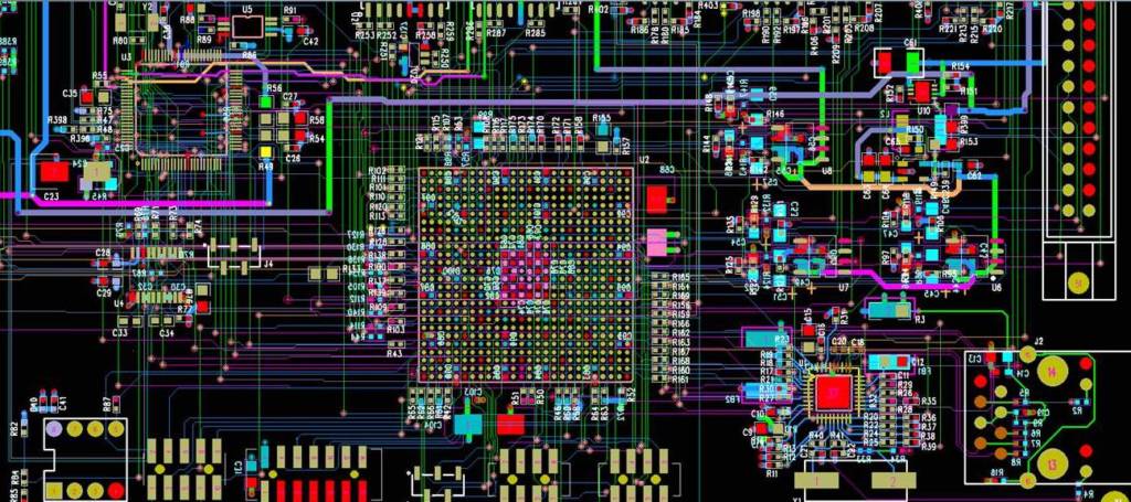
Developing a High-Speed PCB Schematic
One of the first steps of designing a PCB is to create a schematic, which refers to the design at the electrical level of the board’s purpose and function. A schematic is essentially a map or blueprint that includes all the layout details, such as impedance signals, component placement, inputs/outputs, etc.
No matter what type of PCB you have, it’s important to get the design and layout right the first time. If not, you could face routing problems, EMI interference, and signal integrity that may result in project delays.
Important Components of a High-Speed PCB Design
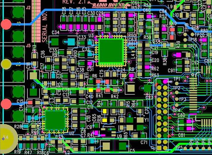
Component Locations and Power Supply Biasing
A component refers to all parts that are used in building any electronic equipment, such as resistors, capacitors, amplifiers, and processors, to name a few. Following the schematic diagram closely for the component placement is critical to avoid costly or untimely schedule interruptions.
If you have bypass capacitors or resistors to keep the noise of the PCB down, you want to place them next to the power-supply pin. Don’t string them along the bottom. In order for these types of components to do the work for which they are intended, the components need to be near the devices power input pins that relate back to the schematic diagram.
Return Path Design
The current return path is a path through which electrons flow from a voltage or current source. The “source” of electrons is the point where they enter into the circuit. And the point where electrons leave an electrical circuit is called the ‘return’ or ‘ground.
Parasitics
This refers to unwanted signal or power integrity, which can add unwanted noise. You can avoid this problem by using signal models and ground power models, the correct materials, and referring to IPC layout guidelines for additional information.
Signal Routing
You want to follow the schematic as closely as possible. Follow the rules when it comes to differential and single-ended pairs.
Shielding
This refers to protection for sensitive circuits from internal and external interference — in other words, outside noise.
High-Speed PCB Design Guidelines
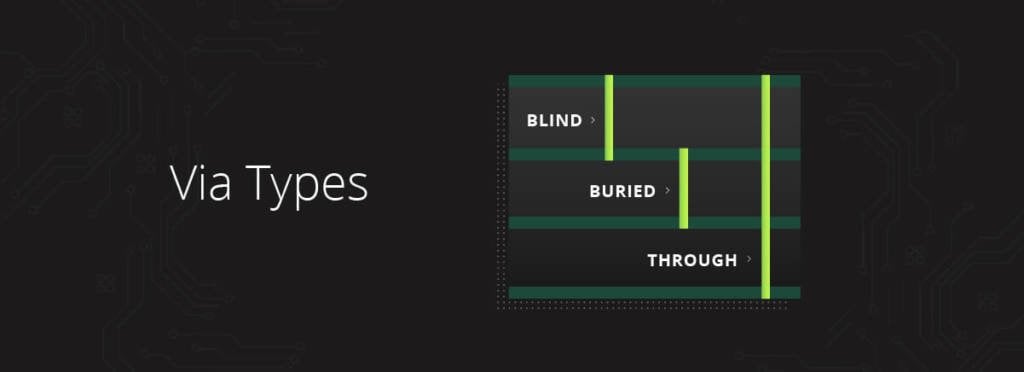
- Minimize use of vias – When it comes to differential pairs, you’ll want to minimize the use of vias from going up and down through the board.
- Use length equalization when necessary – Have differential pairs or signal pairs matched in length so that the timing of the circuit traveling down the copper trace will be the same.
- Prefer shorter trace lengths – In general, you want the trace length to be close and short to the device they are powering.
- Pay attention to trace spacing – This minimizes unwanted noise and interference.
- High voltage currents – IPC has specific rules regarding high voltage currents and signal trace spacing.
Need Help With Your Next High-Speed PCB Design?
Cirexx has dedicated engineers and operators who have the experience and knowledge to answer all of your high-speed PCB questions and help you avoid any unnecessary project delays and pitfalls. We use the latest software and technology, a secure network, and our own streamlined processes to deliver exactly what you need when you need it.
If you have any questions or would like more information, please contact us or request a quote today!