PCB Manufacturing Process [Step-by-Step Guide]

Printed circuit board fabrication and manufacturing has certainly evolved over the last few decades with the addition of new types of technology and manufacturing equipment. But one thing has remained the same — the process is often a complex and intricate one, and regardless of the type of PCB, proper manufacturing is essential to the board’s success and ability to function.
PCB Glossary of Terms
Before we begin, here are some of the most common terms used during the manufacturing process.
- Copper is a highly conductive element used to make the signal traces that conduct electricity.
- Etching refers to the action of removing unwanted excess copper from the copper layer.
- Lamination is the process of thermally laminating layers together. There are two main types — vacuum lamination and sequential lamination. Sequential lamination refers to the process of laminating two consecutive layers together. Vacuum lamination is a process in which air is extracted during the lamination process to prevent internal voiding in the circuit board or flex.
- Plating is a process where copper metal is electroplated onto the image of the PCB in order to plate through-holes.
- Laser drilling refers to the process of creating via-in-pad holes in the PCB.
- Silkscreen, known as a “silkscreen legend,” refers to the decals and reference designators in epoxy ink printed on a PCB. A silkscreen will help you recognize warning symbols and identify components and where they are to be placed. A silkscreen will also identify test points and manufacturer marks and more. The ink is typically white, and black may also be used at times when the substrate is white in color. The ink is digitally printed and doesn’t impact the function of a PCB, but it’s an equally important part of a PCB’s construction.
- Soldermask is a technique in which all parts of a circuit board are coated with epoxy except the contacts to be soldered, the gold-plated terminals of any card-edge connectors, and fiducial marks.
- Substrate refers to the base material used in a PCB.
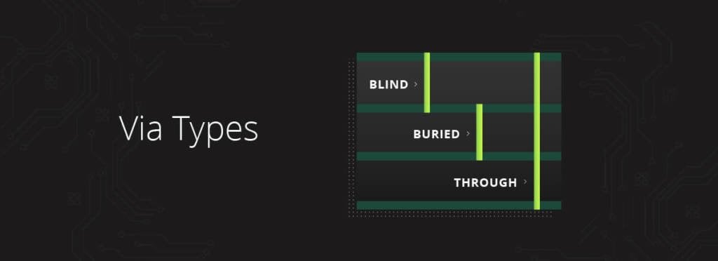
- Via fill is a technique that completely closes a via, also known as a vertical interconnect access. A via is a plated-through hole in a PCB that is widely used to route a trace vertically in the board from one layer to another. Vias are typically filled with epoxy or another type of non-conductive material. A copper via electrolytic fill is used for blind vias.
Step-by-Step Guide Manufacturing Process for Multilayer PCBs
Now let’s go through each step of the PCB manufacturing process. It’s important to note that this guide pertains to all types of PCBs, but there may be slight variations with each step depending on the category of board.
- Define the substrate based on environmental and electrical requirements.
- Print the inner copper layers.
- Etch the inner layers.
- Perform an automatic optical inspection (AOI).
- Align the layers.
- Laminate the layers together.
- Drill holes into the PCB.
- Perform outer layer imaging.
- Plate the PCB.
- Etch the outer layers.
- Apply the soldermask.
- Apply the silkscreen.
- Apply the PCB surface finish.
- Conduct an electrical test.
- Conduct a final inspection.
You first need to select what type of substrate material you will use for manufacturing. The choice of substrate and other materials will depend on the type of PCB and other parameters such as signal integrity,signal speed, and the environment in which it will be used.
For example, single layer PCBs are made out of a single layer of substrate; one side is laminated with a layer of metal — typically copper. With double layer PCBs, both sides of the substrate have a metal layer. Multi-layer PCBs contain three or more copper conductive layers.
A copper-clad substrate or polyimide-based film is used for flex circuits, and for rigid-flex circuits. Another substrate option includes Teflon (PTFE).
During this step, photoresist is laminated to the copper surface(s), and the image is scanned onto the photoresist; it then goes through a developing process where the image is created for the next step in the inner layer of etching. Outer layers have the same process followed by electroplating.
The etching process then removes the unwanted, excess copper from the copper layer.
The process of AOI involves using a specialized machine to check the PCB for possible errors and defects that are otherwise hard to detect with the human eye.
At this point, the engineer will ensure all PCB layers are properly aligned prior to any type of lamination.
During this process, the engineer thermally laminates the layers together. The type of lamination will depend on the base material specified and thermal and pressure requirements of the material.
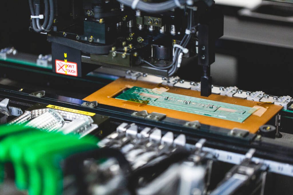
The engineer uses an X-ray machine to find the drill spot locations, and drilling is completed using computer-guided equipment.
The engineer electroplates copper metal onto the surface of the PCB in order plate through-hole and or blind vias. The type of plating will also depend on the function of the printed circuit board. Plating options include, plated edges, plated radii (castellation), and plated cutouts.
This refers to a process where after the etch resist (tin) is plated on the exposed circuitry, the photoresist is stripped and the product then is transported through the etching equipment where the exposed copper is etched away.
At this stage, the PCB is coated with epoxy except for the contacts to be soldered, the gold-plated terminals of any card-edge connectors, and fiducial marks.
Any decals and reference designators are printed in epoxy ink on the PCB. This information may include warning labels, manufacturer logos, or other numbers and information.
A PCB surface finish has two main functions — to prevent the copper from oxidizing and to provide a solderable surface — and the type of finish will depend on the purpose of the PCB. There are nine main PCB surface finishes with electroless nickel immersion gold (ENIG) being the most popular.
During this stage at the end of the process, a technician will perform a flying probe electrical test to ensure the PCB is functional per the IPC-356 nest list requirements.
Upon completion of an electrical test, an engineer will perform a complete quality control/quality assurance inspection, looking specifically at drawing requirements, impedance requirements and whether the product meets IPC Class 2 or Class 3 specifications
Questions About the PCB Manufacturing Process?
We’re ready to provide you with answers. The industry has changed, and we’ve adapted, which means we keep up to date on the latest PCB technology and equipment. If you have any questions about PCB fabrication and manufacturing, please contact us. If you’re ready to get started on your next project, just submit a request for a quote, and we’ll be in touch.