Your Complete Guide to PCB Assembly

There’s a lot that goes into the design and fabrication of a printed circuit board, but the assembly process is just as important. If you aren’t using a reputable provider who follows best practices, your project could end up facing costly delays.
Keep reading to learn more about the entire PCB assembly process — including a step-by-step guide.
PCB Assembly Basics: Designing a Board for Success
Printed circuit board assembly (also known as PCBA) is the process of mounting a fabricated board with the correct components. But you can’t assemble a board if it isn’t designed correctly.
First, let’s explore the typical makeup of a printed circuit board, including materials and components.
- Substrate — This refers to the supporting material that holds the components and traces.
- Copper — This element is used in printed circuit boards due to its highly conductive electrical components.
- Solder mask — This is a technique in which all parts of a circuit board are coated with epoxy, except the contacts that need to be soldered, the gold-plated terminals of any card-edge connectors, and fiducial marks.
- Silkscreen — Though this doesn’t impact a PCB’s function, it’s worth mentioning. A silkscreen refers to digitally printed legend that outlines the decals and references designators in epoxy ink printed on the board. A silkscreen will help you recognize warning symbols and identify components and where they should be placed.
- Annular ring — This refers to the copper ring surrounding the holes on a board.
- Trace and space — A trace is the copper structure that the signals travel through — commonly referred to as a wire.
- Thru-hole or surface mount components — Components refer to any basic part that is used in building electrical equipment, such as resistors, capacitors, fuses, etc.
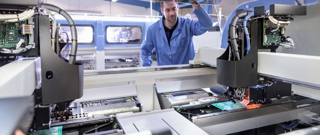
PCB assembly equipment varies and will depend on the provider you choose.
Now let’s quickly review the PCB design basics.
- Understand electrical parameters. This includes current maximums, voltages, signal types, impedance characteristics, and more.
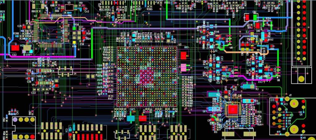
- Create the schematic. A schematic refers to the design at the electrical level that details the board’s purpose and function.
- Use a schematic capture tool to create your PCB layout. Software platforms such as Mentor PADS®, Allegro, or Altium will show you exactly how your board will operate and where the components will be placed.
- Design PCB stackup. A stackup refers to the number of layers and corresponding materials of the board.
- Define design rules and requirements. This step is largely dictated by standards and acceptability criteria from the IPC, which is the industry association for PCB and electronics manufacturing.
- Place components. In most cases, you will discuss design and layout guidelines with your PCB provider when it comes to the placement of components.
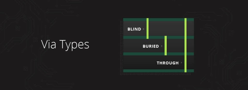
- Insert drill holes. This step is driven by the components and a connection.
- Route the traces. This refers to connecting segments of the path.
- Add labels and identifiers. Now is the time to add any labels, identifiers, markings, or reference designators to the layout.
- Generate design/layout files. These files contain all the information related to your printed circuit board. Once they are generated, your PCB is ready for fabrication and assembly.
Step-by-Step PCB Assembly Guide
There are several different types of assembly, depending on the components of your PCB:
- Thru-hole — Components are inserted through holes in the circuit board and then soldered.
- Surface mount — Surface mount technology (SMT) is an assembly method in which components are surface mounted or placed directly onto the surface of the PCB. This is the most common type of PCB assembly.
- Mixed technology — This is a combination of thru-hole and SMT.
- There is also the functional test that must be accomplished.
- Burn-in is a process where the board is energized and under operation for a specified amount of time.
- Electro-mechanical — This involves assembling into an aluminum structure and is also known as a “box build.”
- Wire harnessing — This involves all of the internal electrical connections in the box.
PCB providers may also provide a variety of assembly services. These include:
- Turn-key — The PCB provider will buy the parts.
- Consigned — You have the option to buy the parts yourself.
- Partial — This is a combination of turn-key and consigned.
There are different types of assembly, depending on the purpose and function of your circuit board, but here is a general overview of what you can expect:
- Complete a design for manufacturability check.
- Apply solder paste to the printed circuit board.
- Move the PCB to SMT equipment that will place components on the board.
- Undergo “reflow” soldering on the board, which is typically IR or vapor phase.
- Inspect the board for quality control purposes, which can be visual or through an Automatic Optical Inspection (AOI).
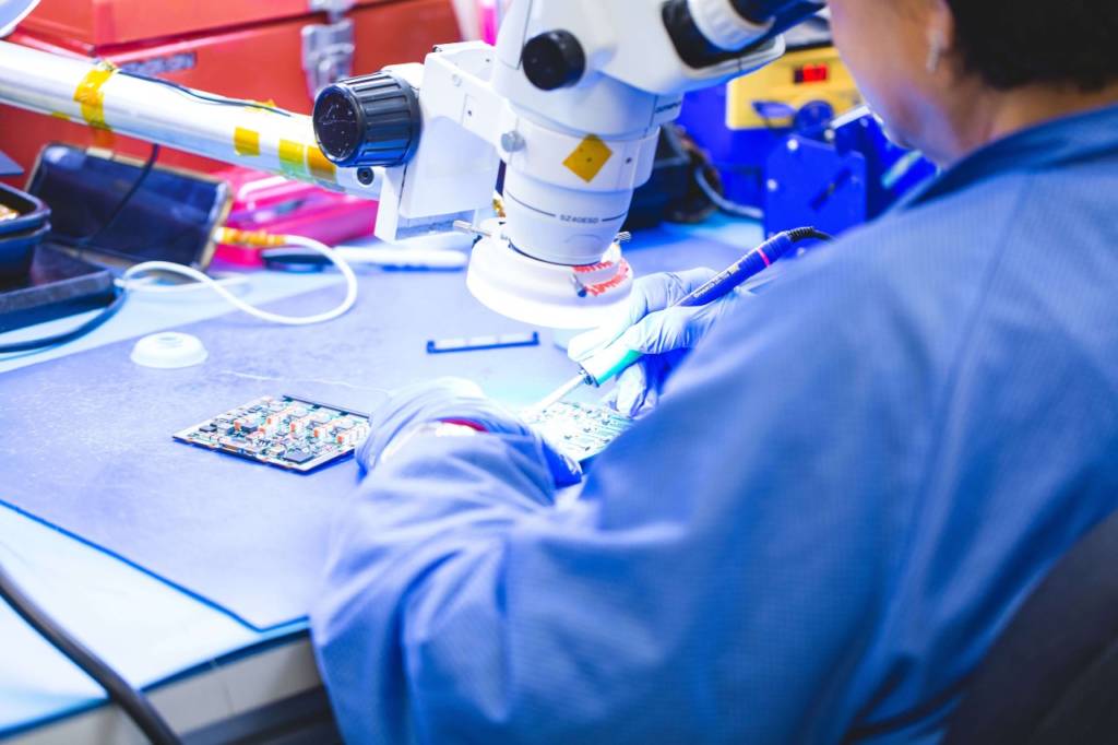
- Insert and solder through-hole components, if necessary.
- Complete a final inspection, which can be visual or through AOI.
PCB Assembly Best Practices
One of the most important aspects of the PCB assembly process is timely, thorough communication with your PCB assembly partner. At the beginning of the process, you and your PCB provider should establish the main points of contact and decide how often (and through which channels) you will communicate during the process.
This is critical since failure to properly communicate can result in delayed timelines and unnecessary expenses.
Cirexx’s PCB Assembly Capabilities
The PCB assembly process can seem complicated — but our experts can help. We differentiate ourselves by being able to take on even the most complex jobs — all the way from layout through assembly — and we do this under one roof with state-of-the-art technology and a top-notch engineering and assembly operator team. We specialize in best practices for flex and rigid-flex PCB assembly, and our certified operators understand how to properly treat and assemble flex circuits to avoid delamination. Contact us if you have any questions or would like to request a quote for your next project.