Determining PCB Via Size [w/ Guidelines]

A via is an essential component of any printed circuit board (PCB), but there are specific requirements and guidelines you should consider when selecting the right via size for your next project. Failure to do so may result in unnecessary delays and costs.
Keep reading for details on PCB via size, including the different types, standard sizes, requirements, and considerations to keep in mind when designing your next project.
What Is a PCB Via?
A vertical interconnect access (or via) is a plated-through hole in a printed wiring board that is used to route a trace vertically in the board from one layer to another. Through-hole vias can be drilled mechanically, and blind vias are drilled with a laser.
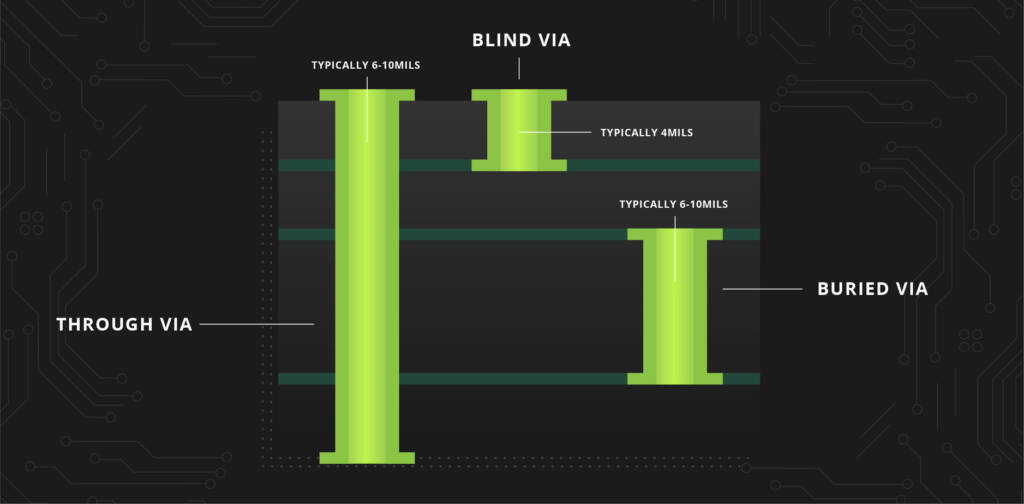
PCB Via Types
There are three main types of PCB vias:
- Buried via: A buried via is needed when you have what is commonly referred to as sequential lamination (or multi-lamination) projects.
- Through via-in pad: A through via connects the two exterior layers by drilling all the way through from the top to the bottom layer.
- Blind via in-pad: This via refers to a laser that only goes from one layer to the next.
Via Type vs. Via Size
PCB Via Type vs. Size |
||
Via Type |
Function |
Size Criteria |
| Blind via in-pad | Connects directly to the layer below | 004” to .006” after drilling |
| Buried via | Varies — but must not be less than .008” after plating to facilitate conductive or non-conductive epoxy via fill | Not less than .008” after plating and not more than .018” after plating |
| Through via in-pad | To connect top and bottom layers | Same as above. Pad size must be taken into consideration to meet annular ring requirements |
Standard Via Sizes
The most common via size is 10 mil, which is 7 mil after plating, but via size typically depends on the thickness of the board and is considered an aspect ratio equation. Micro vias, both laser drilled and mechanically drilled 4 mil holes, are related to the thickness of the boards. Laser drilled vias, on the other hand, have a requirement to have 3 mils of dielectric spacing between layers.
PCB Via Size Requirements
Size requirements are typically dictated by IPC standards and guidelines. IPC is a nonprofit association for electronics and manufacturing and “leading source for industry standards, training, industry intelligence, and public policy.”
It’s essential to always follow IPC guidelines for PCB technology, which include stipulations such as distance between vias. IPC design guidelines for Class 2, Class 3, Class 3ES, and the military are especially important because they all differ slightly.
Guidelines & Considerations for PCB Via Size Selection
In addition to consulting IPC guidelines, keep these questions and considerations in mind:
-
- Via type. Which is right for your project? If you have one lamination with no via fill or technology, you will have a lot of room for larger holes.
- Via size. This depends on the thickness of the board (also known as an aspect ratio equation).
- Via tolerance. It’s important to specify hole size tolerance, but PCB providers often provide in-house guidelines.
- Supporting the appropriate technology. When you need blind or buried vias, consult with your PCB supplier to begin developing a stack-up that supports that technology.
- Annular ring. Be mindful of annular ring requirements per Class 2 and Class 3.
- Board IPC classification. Class 2 and Class 3 boards have different specifications in terms of tighter tolerances and requirements.
- Equipment capabilities. Make sure you work with a PCB manufacturer who has invested in the newest equipment and technology. Many providers do not have the appropriate capabilities in house and are forced to subcontract the work to a third party.
- Board density. This metric can influence the selection of via diameters.
- Via filling procedures and plating applications. Filling a via must prevent the entrapment of chemicals or other substances within the holes, which can eventually cause defects to the printed circuit board. Vias are filled with conductive or non-conductive epoxy paste. Blind vias and via in-pads are filled with specially designed electroplating chemistry.If you are looking to move heat from one side of the printed circuit board to the other, you will likely opt for a conductive fill.
Vias must be sealed or covered by capped plating. The combination of the sequential build-up of technology and the mechanical processes can disturb the buried via plating, resulting in problems with the board. To prevent this problem, the vias are filled with resin before being plated.
A via in-pad must be plated over because you are placing a component on the pad.
Additional Questions About PCB Via Sizes?
We have the answers. Cirexx is your best-in-class solution for PCB layout, fabrication, and assembly. With more than four decades of experience, we have manufactured PCB layouts for almost every leading technology company, and we’ve worked with industries all over the world. Contact us today for more information or to connect with our sales team.