RF/Microwave PCB Design & Layout Guide

Radio frequency (RF) and microwave PCBs are popular circuit boards that require specific design and layout considerations. In this guide, discover what constitutes a successful RF/microwave PCB project, including design considerations, material selection, integral components, and more.
What Are RF and Microwave PCBs?
Transmission Lines and Impedance
Integral Components
Layout Techniques and Strategies
Materials and Board Stackup
Skin Effect and Loss Tangent
Shields and Shielding
PCB Materials, Fabrication, and Assembly
What Are RF and Microwave PCBs?
RF and microwave PCBs operate on signals in the megahertz to gigahertz frequency ranges (very low frequency to extremely high frequency), which are commonly used for communication signals in everything from cell phones to military radars. In terms of layout, fabrication, and assembly guidelines, RF and microwave PCBs are one and the same.
Transmission Lines and Impedance
A transmission line refers to wires or conductors that move energy from one point to another. They are structures of copper that carry electrical signal through PCB without interruption or noise and protection from electromagnetic interference (EMI).
There are many types of transmission lines, including:
- Micro strip
- Strip line
- Surface micro strip (copper trace will run on the surface)
- Edge couple surface micro strip
- Edge couple symmetrical strip line
- Embedded micro strip
- A strip line is typically embedded, whereas a micro strip sits on the surface. Co-planar is also another type of transmission line.
All the structures of a transmission line will carry impedance.
Integral Components
The exact components will vary based on the particular PCB, but the following list details important components typically found in an RF/microwave PCB design:
- Amplifiers
- Bluetooth circuits
- Antennas
- Inductors
- Capacitors
- Resistors
- Filters
- Couplers
- Copper
Layout Techniques and Strategies
You will need to know what impedance you will carry through the transmission line, which also directly relates to your choice of PCB materials. An engineer will help determine what type of transmission line is needed.
The layout of an RF/microwave PCB is typically a transmission line on top with a copper trace followed by dielectric materials. The second layer is either a ground plane or power plane. All of this directly affects the impedance of the transmission line, the width of the copper trace, and the height of the material on the circuit board.
Noise is one of the most important concerns with RF/microwave layout. These types of PCB are usually fabricated with a digital power supply, which means they can be noisy. It’s important to isolate the part of the circuit that’s a radio frequency to avoid this type of interference. In some cases, you can protect the circuit from noise with space; other times a ground barrier or shield around the circuit is needed.
Materials and Board Stackup
RF and microwave PCBs are typically built using advanced composites with very specific characteristics for dielectric constant (Er), loss tangent, and co-efficient of thermal expansion (CTE).
High frequency circuit materials with a low stable Er and loss tangent allow for high speed signals to travel through the PCB with less impedance than standard FR-4 PCB materials. These materials can be mixed in the same stackup for optimal performance and economics.
It’s important to consider impedance calculations, which go hand in hand with material selection. Two-layer boards are relatively simple, but multi-layer PCBs can prove more challenging. For example, transmission lines and ground planes must be next to each other in the stackup of an RF/microwave PCB. If they are two layers away from each other, the software used by the engineer will help develop the correct stackup to determine the height and weight of all the layers together.
Some materials work better with RF/microwave PCBs than others, but it depends on the frequency. Teflon, for example, works well with high frequency PCBs because it has a low loss tangent.
Skin Effect and Loss Tangent
Skin effect refers to noise that is picked up on the board due to the copper trace. Loss tangent is the measure of dielectric loss due to electromagnetic energy. High frequency circuit materials with a low stable Er and loss tangent allow for high speed signals to travel through the PCB with less impedance than standard FR-4 PCB materials.
RF/microwave PCBs typically use materials with a lower loss tangent.
Shields and Shielding
The return path on a circuit must be protected, or “shielded,” from noise. A shield could refer to a physical shield or the placement of the components. Adding vias is also another consideration that could help avoid noise and interference.
RF/Microwave PCB Materials, Fabrication, and Assembly
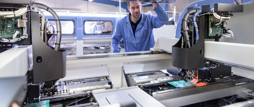
Cirexx’s engineers have extensive experience dealing with the vast amounts of materials related to RF and microwave technology, which helps ensure your orders are designed for manufacturability while being produced on time and on budget. We can provide custom RF and microwave PCB fabrication in as little as 24 hours — all you have to do is ask. Plus, all the design, fabrication, and assembly are done under one roof with no outsourcing.
If you have questions or would like more information about RF/microwave PCBs, please contact us or request a quote.